Utkaarsh Gupta

Analog design · Analog layout
Final year · KLE Tech, Hubballi

Utkaarsh
Gupta

ECE undergraduate at KLE Technological University, Hubballi, graduating 2027. I design CMOS analog circuits in Cadence Virtuoso and draw their layouts by hand.

Work

Six projects. Each one opens with the real files: schematics, layouts and simulation results from Cadence.

  1. 01CMOS synchronous buck converterAnalog · power2026
  2. 02Standard-cell libraryLayout2026
  3. 03Two-stage op-ampAnalog · layout2026
  4. 04Conference paper, NKCONPublication2026
  5. 05Smart agriculture for hill farmsHackathon · embeddedSIH
  6. 06IC packagingCadence AllegroNow

The library

Every cell he saved in Cadence, opened from the project folders: 20 cells, 37 views. Full Virtuoso captures where they exist; the preview Virtuoso stored, otherwise.

Library Manager

Library

    Cell

      View

        01

        CMOS synchronous buck converter

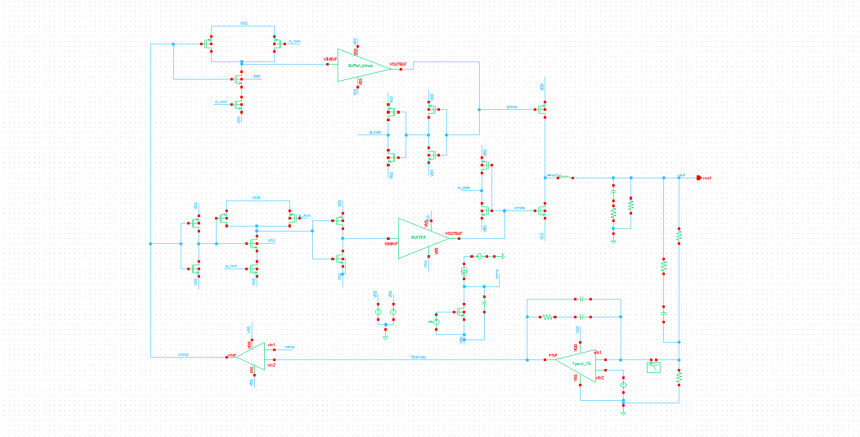
        A closed-loop DC-DC converter that turns 3.3 V into a regulated 1.8 V at 100 mA, designed at transistor level to a specification from Green PMU Semi. Every block below, from the op-amp to the gate drivers, is a real circuit in the Cadence library.

        Process
        UMC 180 nm
        Tools
        Virtuoso 6.1.8 · Spectre
        Role
        Led the design, team of 4
        Specification
        Green PMU Semi
        Guide
        Dr. Sujata Kotabagi
        When
        Feb – Aug 2026
        • 1.80 Voutput, from 3.3 V
        • 26.7 mVripple, peak to peak
        • 0.75 mssettling from power-on
        • 1 MHzswitching
        • 89.3 %efficiency, calculated
        • ≈ 80 dBerror-amp gain

        Run it

        The converter, running live in your browser. Pick an experiment: each one starts from the working design, changes one thing, and tells you what to watch.

          Free play: click a on the schematic to probe that node, or a block to remove it.

          Channels

          A behavioural model with the design’s component values, simulated at 5 ns steps. It shows how the circuit behaves; the Spectre results are further down.

          Block by block

          Pick a block to see what it does, next to the actual schematics and simulations from the Cadence library.

          From the library

          Results

          Spectre transient simulation of the full transistor-level design, final run 2 July 2026, 18 Ω load.

          Input voltage3.3 V
          Output voltage1.80 V 1.7876 – 1.8143
          Output ripple26.7 mVpp
          Load current100 mA
          Settling time0.75 ms
          Switching frequency1 MHz
          Conduction modeCCM
          Efficiency89.3 % calculated from losses
          Error-amp DC gain≈ 80 dB
          Dead-time10 – 12 ns
          L / C7 µH / 7 µF ESR 50 mΩ
          VOUT from power-on, 0–10 ms
          Steady-state ripple, markers 26.7 mV apart

          How it got there

          The cells in the design library show the path: ideal models first, then open loop, then the real op-amp in three revisions, then the closed loop.

          Converter
          1. ideal
          2. ideal_openloop
          3. ideal_buck
          4. open_loop
          5. open_loop_new
          6. Open_Loop_R
          7. buck_ready_fast
          8. buck_end
          Op-amp
          1. 7_Pack
          2. 7pack_76db
          3. 7_pack_80db
          4. 7_pack_final
          Blocks
          1. Buffer
          2. buf_new
          3. type3_comp
          1. Spec arrives3.3 V in, 1.8 V out, 100 mA, from Green PMU Semi.
          2. On paperDuty cycle, ripple, L, C and loop crossover by hand.
          3. First open loopL 24.2 µH, C 10 µF, PMOS 50 µm, NMOS 5 µm.
          4. The op-amp76 dB, then 80 dB, then final; stable inside the loop.
          5. Loop closesRegulates; start-up dips to 1.25 V.
          6. Final1.80 V, 26.7 mV ripple, 0.75 ms; L 7 µH, C 7 µF.
          7. Written upReport, poster, conference paper.
          02

          Standard-cell library

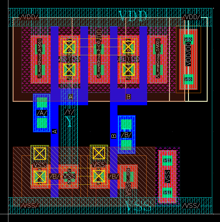
          Five logic cells, each drawn from its transistor schematic to a full layout in Virtuoso Layout XL, then checked against the foundry’s design rules (DRC) and against the schematic (LVS).

          Process
          UMC 180 nm
          Tool
          Virtuoso Layout XL
          Cells
          INV · NAND2 · MUX2 · XOR2 · OAI311
          Checks
          DRC ✓ · LVS ✓, all cells
          Variants
          OAI311 in M1 and M2 routing
          Work
          Individual

          How a cell is built

          A layout goes down one mask layer at a time. Here is an inverter, redrawn: click a layer, or build it in order.

            03

            Two-stage op-amp

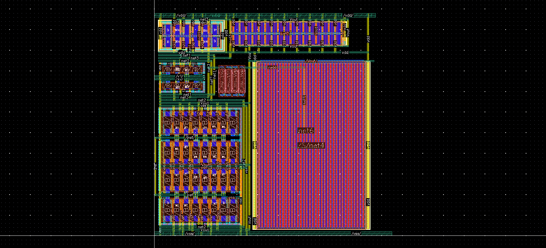
            A two-stage Miller-compensated op-amp, nicknamed the “7-pack”. It is the error amplifier of the buck converter, and a second copy serves as its PWM comparator. Taken from schematic to full layout.

            Topology
            Two-stage, Miller
            DC gain
            ≈ 80 dB
            Bias
            20 µA reference
            Miller cap
            2 pF
            Revisions
            76 dB → 80 dB → final
            Checks
            DRC ✓ · LVS ✓
            Schematic, with device sizes
            Layout, compensation capacitor array on the right · hover to inspect
            The 80 dB revision

            More

            04

            Publication · submitted

            Design and Simulation of a CMOS-Based Synchronous Closed-Loop DC-DC Buck Converter in 180 Nanometer Technology

            Utkaarsh Gupta, Shashank Dollin, Gouri VK, Archana Hosamani, Dr. Sujata Kotabagi

            NKCON, SECAB University · decision expected late October 2026

            05

            Smart India Hackathon · semi-finalist

            Smart agriculture for hilly regions

            A sensor-equipped canal irrigation system for the terrace farms of Sikkim. Solar and light (LDR) sensing automate watering, cutting power use and manual work.

            06

            Coursework · current semester

            IC packaging in Cadence Allegro

            Wire-bond and flip-chip packaging, working on ball-grid-array (BGA) package designs.

            07

            Industry training · 2025

            Visteon Scholar Program

            Industry training in embedded systems, networking and automotive technologies.

            08

            Leadership · Apr 2025 – now

            Vice-Chair, IEEE Student Branch

            Organises workshops, seminars, hackathons and student activities at KLE Tech.

            Résumé

            One page. Updated October 2026.

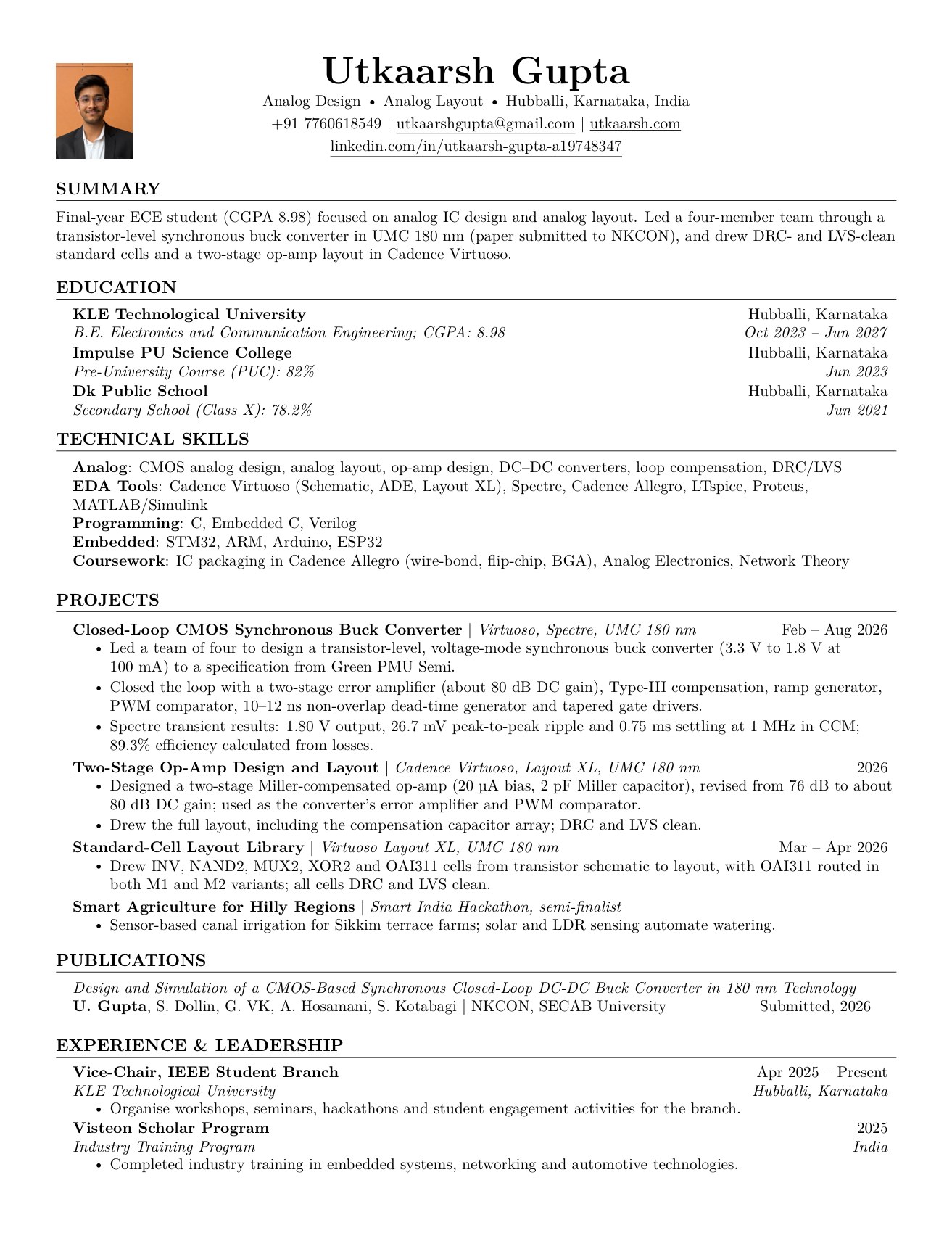
            Résumé of Utkaarsh Gupta, page 1
            Download PDF  Open in a new tab
            Degree
            B.E. Electronics & Communication
            University
            KLE Technological University, Hubballi
            CGPA
            8.98
            Graduating
            June 2027
            Looking for
            Analog design and analog layout roles, internships now
            Utkaarsh Gupta

            Looking for analog design and layout roles.

            Final year, Electronics and Communication Engineering, KLE Technological University, Hubballi. Vice-Chair, IEEE Student Branch. Open to full-time roles from 2027 and internships now.

            Design
            Cadence Virtuoso (Schematic, ADE), Spectre, LTspice, Proteus
            Layout
            Virtuoso Layout XL, DRC, LVS
            Packaging
            Cadence Allegro
            Modelling
            MATLAB / Simulink
            Code
            C, Embedded C, Verilog · STM32, ARM, ESP32, Arduino